Breaking the GPU Paradigm - A Systems Thinker's Guide to Wafer Scale Computing
“What goes around comes around; every challenge demands its own solution.” — Adapted from Guiguzi, an ancient Chinese philosopher
To be honest, the WaferLLM project has indeed come to an end. It was accepted at OSDI, but rather than pure joy, my feelings are more complex. As a skeptic, I still don’t believe that LLMs and the Transformer architecture are the ultimate answer, nor do I think the scaling law curve can continue indefinitely. Standing at this technological inflection point, we need to stay clear-headed more than ever—complacency means stagnation.
The current AI development is like climbing a peak that no one has ever conquered. The path ahead is filled with both unknown challenges and unique breakthrough possibilities. This understanding led me to choose this quote from “Guiguzi” at the beginning:
“Transformation follows circular patterns, each with its own dynamics, repeatedly seeking balance, adapting strategies to circumstances.“
This ancient wisdom about technological evolution perfectly mirrors our research: technological development is like interlocking gears, facing different phases of changing dynamics, requiring continuous exploration of fundamental principles and strategic adjustments based on actual circumstances. WaferLLM’s design philosophy perfectly embodies this concept of the “circle.”
So what is Wafer?
1 What is Wafer?
Simply put, Wafer-Scale Chip is a technology that uses an entire wafer as a single integrated circuit, rather than cutting the wafer into multiple smaller chips.
Looking at the evolution of chip area, from single-core CPUs to multi-core CPUs, and then to specialized accelerators like GPUs and TPUs, what appears as stacking of computing units is actually an ongoing battle between computational demands and physical limitations. As Moore’s Law gradually fails and single-chip area is locked in the 400-800 square millimeter range, this contradiction becomes increasingly acute under the dual constraints of lithography technology and yield rates.
Wafer-scale integration technology breaks through this deadlock, increasing chip area by two orders of magnitude. Take the Cerebras WSE-2 as an example: with its ultra-large size of 215mm×215mm (46,225 square millimeters), it achieves a hundred-fold area breakthrough compared to traditional GPU chips, integrating 2.6 trillion transistors and 850,000 AI computing cores, breaking through the “area bottleneck.”
1.1 Advantages of Wafer-Scale Technology
From Table 1 in our paper, we can see that wafer-scale chips have several significant advantages over traditional system-level packaging:
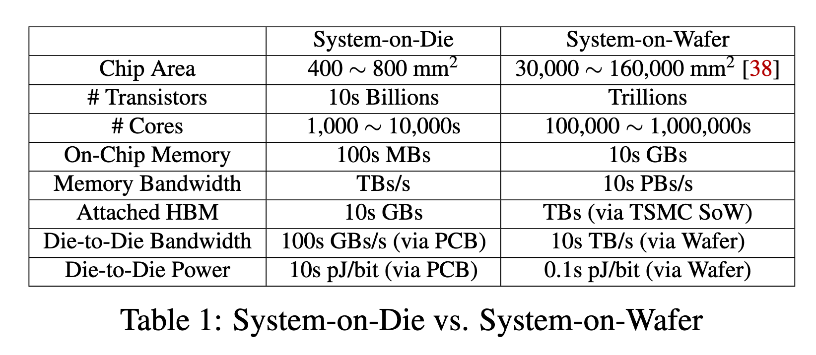
- Performance advantages: Wafer-scale chips can integrate trillions of transistors, 100 times more than common GPUs, supporting millions of computing cores. Meanwhile, the larger chip area also provides tens of GB of on-chip memory and tens of PB/s memory bandwidth, which is over 1,000 times that of standard GPUs.
- Integration efficiency: Wafer-based die-to-die interconnects provide 10x bandwidth per unit area, and compared to traditional PCB connections (like NVIDIA NVLink), there’s nearly 100x improvement in energy efficiency per bit.
- Cost reduction: Wafer-scale integration can reduce manufacturing costs because 30-50% of chip manufacturing costs are related to testing and packaging individual chips. Additionally, companies like TSMC are developing technologies to integrate tested chips onto a single wafer, further improving yield.
In short, we’re trying to follow the traditional multi-core approach and further increase chip area. The above talking points actually come from Wikipedia and other easily accessible resources. It seems like we’re just using better chips and reaping hardware benefits.
But is that really the case?
1.2 Challenges with Wafer
But if we’ve designed chips with larger areas that release more computing power, what’s the cost? After all, there’s no free lunch. Behind every breakthrough lies new constraints.
The cost here is: most of our previous algorithm designs will no longer be applicable.
First, let’s look at how we previously programmed and designed models.
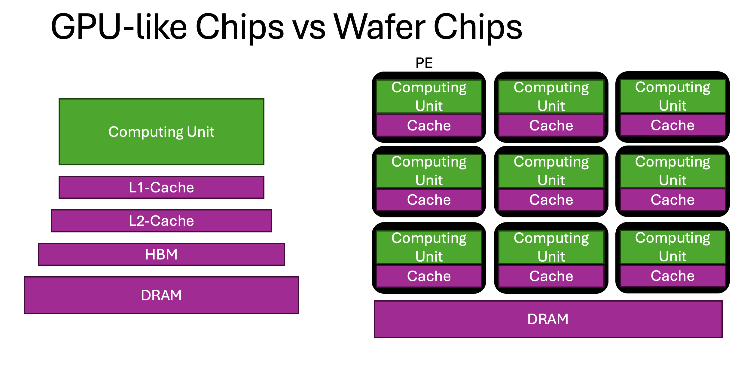
In traditional chip structures, whether CPU or GPU, for a single accelerator, our design approach is closer to Uniform. When designing, we concentrate computing cores together, and with the distance from computing cores, we set up multi-level caches for more efficient memory access.
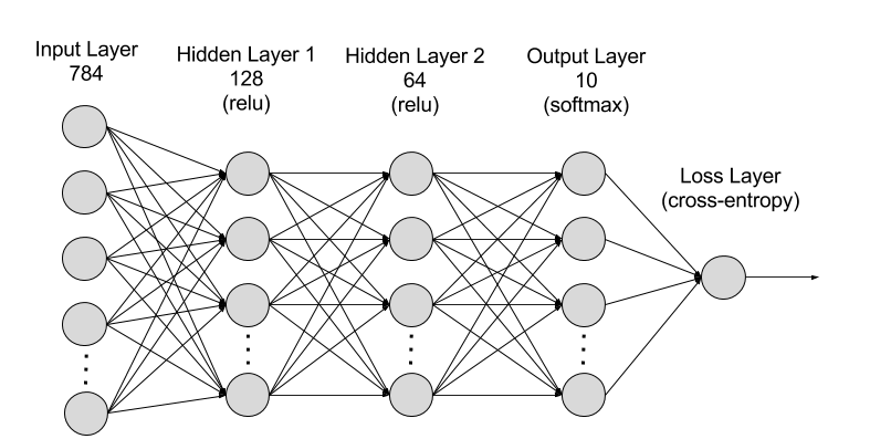
Now, turning from hardware to models. Let’s use the simplest DNN example, MNIST digit1 recognition :
1 | |
We’ve probably seen model structure diagrams like this countless times 2,
When we program and design models, our thinking objects are operators and modules, and we practically never consider data placement issues. We don’t think about where each matrix, h1, h2 is placed on the GPU. Most of the time when we think, we only care about what data is in GPU RAM. So when models with special computation-to-memory access ratios appear, like the decode phase in Llama architecture LLM models.
Let’s bring out the LLM decoding code again, using a numpy version of a simple decoding module as an example, referencing the llama3.np project . We can see codes3 like :
1 | |
In our model design process, we also rarely consider data placement for each part.
More specifically, for example:
- In the three consecutive computation steps of
xq,xk,xv, ournorm_xactually needs to be kept as close to the computing units as possible - After computing
z3, placing it directly in the original location ofz1seems to bring many improvements
Of course, there are more optimization points, which I won’t elaborate on here. Our current solution, as you’ve probably guessed, is Triton. Indeed, we can customize very high-performance CUDA operators and manually manage the complex multi-level memory just mentioned. But Triton provides limited but sufficient programming abstractions, solving what we care about most and what has the most important impact on performance, namely L1 Cache behavior. For LLMs, this step is undoubtedly the most critical for performance, and the Flash Attention series of work discovered the performance bottleneck here and proposed high-performance optimizations.
On GPUs, we’re already unable to handle complex memory management. So when it comes to LLM inference on Wafer, the main challenge is that chip memory becomes even more complex, making the problem even harder to solve. Let’s first look at the structure of the Cerebras chip 4.
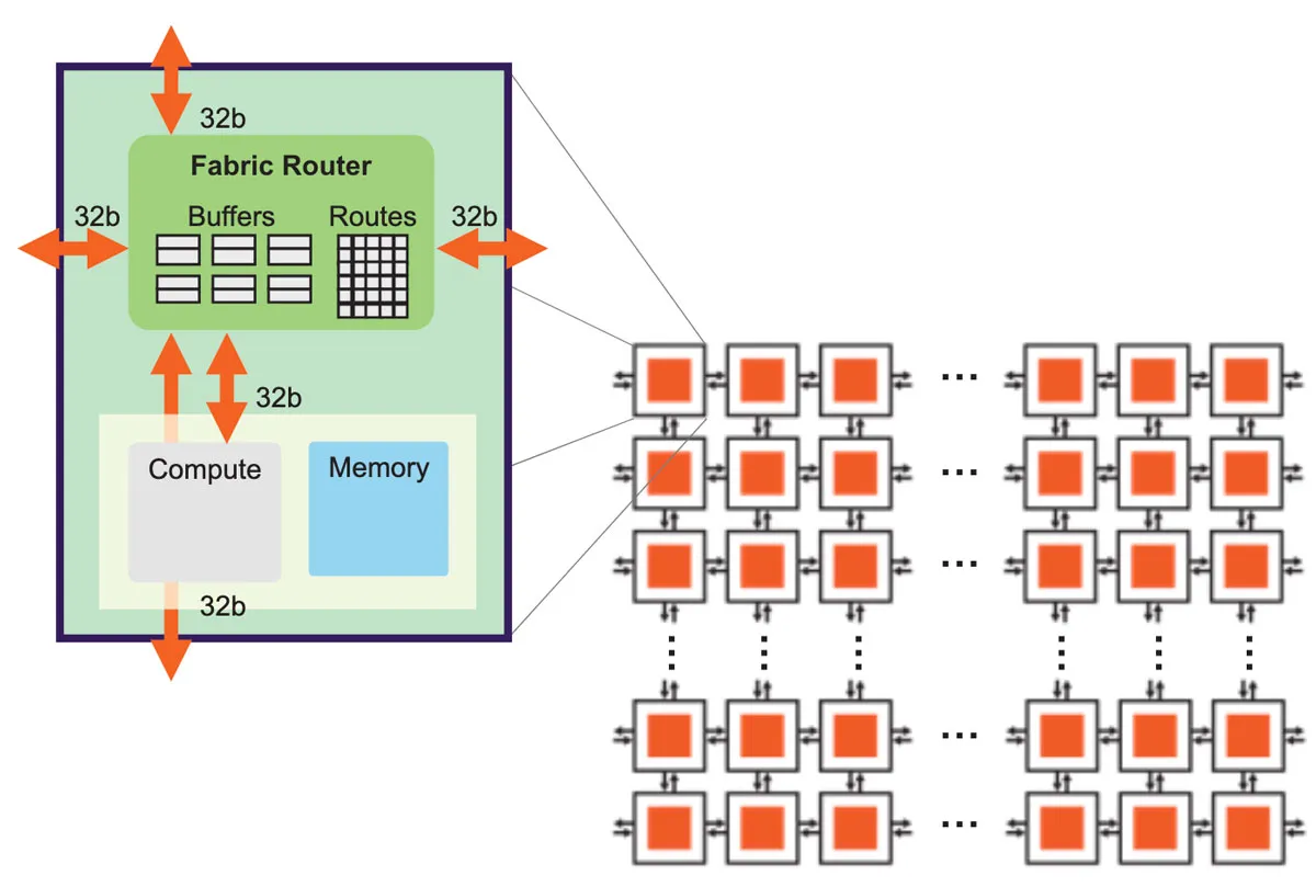
Cerebras’s Wafer Scale Engine (WSE) adopts a unique 2D mesh architecture design, where the entire chip consists of tens of thousands of processing elements (PEs) arranged in a grid pattern on a single silicon wafer. Each PE contains three key components: a compute kernel responsible for actual computation, a small local memory for data storage, and a router for handling communication needs. These PEs are interconnected through a high-performance Network-on-Chip, forming a high-bandwidth, low-latency communication network that enables efficient data flow between different processing units.
- Distributed memory structure: Our memory is fragmented into countless small pieces of on-chip Local Memory (corresponding to GPU’s L1). Individual space is extremely small, for example, only 48 KB on CS-2.
- Mesh NoC: Here we see a 2D Mesh network structure, where accessing data requires complex traversal.
- Data movement overhead: In traditional GPU memory, we rarely care about operations like transpose, slice, reshape, but here any data storage and management becomes exceptionally complex.
So we can see that in such a complex memory structure, even how to cut and arrange model weights becomes a question worth exploring. Not to mention the more complex KV Cache management.
However, in our WaferLLM work, we proposed a complete and feasible solution to all the above problems.
2 PLMR Model
On a Wafer Chip, how many PEs should we use to compute each operator in the model? To write code on a Wafer Chip, the first question we think about is how to map. If there are too few PEs, our parallelism is insufficient and computation becomes the main bottleneck; if we use too many PEs, not only does the number of communications increase, but the communication distance also grows, introducing more communication overhead. Due to current architecture limitations, computation and communication cannot be 100% completely hidden, so the total time overhead has an approximately linear relationship with both. That is, we need to ensure that neither computational overhead nor communication overhead becomes too high.
Therefore, before proposing our algorithms and solutions, we need more precise metrics to guide and evaluate our algorithm design. To address the unique hardware characteristics of Wafer Chips, we proposed the PLMR model, which keenly captures the four attributes we care about most.
2.1 What is the PLMR Model
PLMR is an acronym for four key hardware attributes:
- Massive Parallelism (P): Wafer Chips can easily be equipped with millions of parallel cores, a significant advantage over GPUs’ thousands of cores. Each core has local hardware pipelines that complete data input, output, computation, and memory access in parallel at the cycle level.
- Highly non-uniform memory access Latency (L): Accessing memory on other cores in the grid exhibits highly non-uniform latency. For example, in an N * M grid, the maximum NoC hops to a remote PE is max(N, M). For a million-core on-chip grid, this could reach 1000 hops, so there’s a 1000x latency difference between a PE accessing its own memory and accessing the furthest PE’s memory. Therefore, minimizing long-distance communication is crucial.
- Constrained local Memory (M): Large-capacity memory chips lead to performance and energy efficiency degradation, so each core’s memory is relatively small. Therefore, in our algorithms, all matrices and tensors must be appropriately partitioned so that each PE is allocated small data blocks that can be stored.
- Constrained Routing resources (R): Wafer Chip NoC message sizes are extremely limited (e.g., a few bytes). This limitation requires NoC message headers (like address encoding) to be limited to a few bits, maximizing actual data transfer capacity. Therefore, only limited routing paths can be used, and software systems must carefully plan these paths. We cannot use complex communication patterns without restriction.
2.2 Why We Need the PLMR Model
The PLMR model was proposed based on an in-depth analysis of why existing AI systems cannot fully utilize performance on Wafer Chips. Using the PLMR model, we can analyze why existing AI systems struggle to fully utilize Wafer Chips:
- Shared memory-based systems: Like Ladder, typically assume uniform memory access patterns in the underlying memory hierarchy, unable to tolerate the 1000x latency difference when Wafer Chips access remote memory (violates L). Additionally, these compilers mainly focus on computation while less on optimizing memory and communication constraints, easily leading to massive data copying and violating memory constraint requirements (violates M). Finally, they don’t understand the communication distance of each core, making it difficult to address routing resource constraints.
- Distributed memory systems: Like the T10 system, designed for AI accelerators with on-chip crossbar switches, ensuring constant hop counts for memory access to other cores on the same chip. T10 handles small local memory and balances communication load, addressing memory constraints (M) and routing resource limitations (R). However, on PLMR devices, it cannot consider different hop distances (violates L) and only scales to thousands rather than millions of cores (violates P).
2.3 What the PLMR Model Guides Us to Do
The PLMR model provides the following guidance for designing wafer-scale LLM systems:
- Algorithm design: PLMR inspired us to propose MeshGEMM and MeshGEMV, the first high-performance GEMM and GEMV operators designed for WaferChips.
- Model parallelism strategy: PLMR guided us to design effective LLM parallelism methods for Wafer Chips, including intra-operator and inter-operator parallelism for both prefill and decode phases. This enables WaferLLM to effectively scale to millions of cores (satisfying P) while minimizing communication costs (satisfying L) and memory usage (satisfying M) with simple and limited approaches.
- Memory management and inference engine design: Based on PLMR, we proposed WaferLLM, the first wafer-scale LLM inference system. By running complete LLM inference on a single Wafer Chip, we not only minimize expensive off-chip communication but also maximize on-chip memory bandwidth utilization. We also designed peripheral management settings, including KV Cache management and different weight padding schemes for Prefill/Decode phases.
3 WaferLLM
For LLMs to work on accelerators like Wafer Chips, we need to fully leverage the parallel capabilities of numerous PEs. In both Prefill and Decode phases, we face various challenges.
3.1 Operator Optimization - GEMM
First, in the Prefill phase, we extensively use GEMM, i.e., matrix-matrix multiplication. Traditional matrix multiplication cannot satisfy PLMR constraints.
To determine a scalable distributed GEMM suitable for the PLMR model, we defined the following metrics:
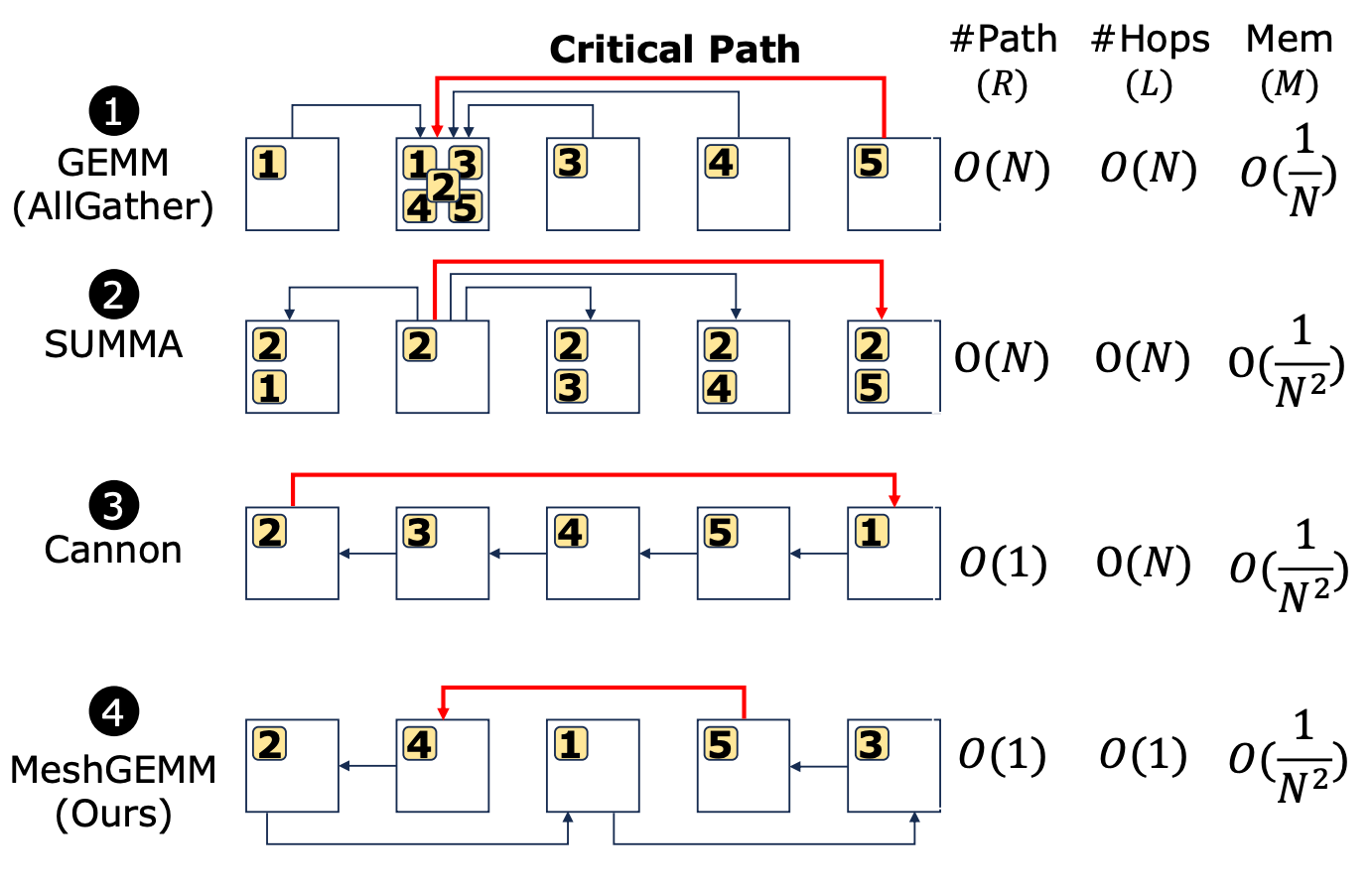
- Paths per core: Number of routing paths per core, fewer paths ensure compliance with R attribute;
- Critical path length: Longest communication path for transferring sub-matrices at each step (red line in the figure above), fewer hops comply with L attribute;
- Memory per core: Memory required per core, lower usage ensures M attribute.
Analyzing existing distributed GEMM methods and showing how MeshGEMM satisfies these metrics:
- Allgather-based GEMM: Common in GPU and TPU clusters. The longest communication path at each step is one core collecting data from the furthest core, requiring N steps to complete allgather. Each core creates N communication paths with neighbors in its row and column (violates R). Each step’s gather spans O(N) hops in the critical path (violates L), and each core uses O(1/N) memory due to inflated work buffers, far exceeding the local sub-matrix’s O(1/N²) (violates M).
- SUMMA: Cerebras’s default algorithm. The longest communication path at each step is one core broadcasting data to the furthest core along a column or row. Each core creates N communication paths (violates R), spanning O(N) hops in the critical path (violates L). While SUMMA improves memory usage, it’s still twice the size of the local partition sub-matrix.
- Cannon: A grid-optimized distributed GEMM choice, popular in supercomputers. The longest communication path at each step is the head core sending data to the tail core. Each core communicates with two neighbors in a 2D ring, requiring only O(1) communication paths and optimal O(1/N²) memory usage. But it produces O(N) hops in the critical path (violates L).
- MeshGEMM (our method): A distributed GEMM that complies with the PLMR model. Each core communicates with two neighbors that are two hops away. This design achieves O(1) communication paths per core and optimal O(1/N²) memory usage similar to Cannon. Crucially, it limits the critical path to 2 hops with O(1) complexity, cleverly addressing the L attribute.
Our design involves two key steps:
- Using GEMM’s cyclic shift process to ensure algorithm correctness
- Proving that two-hop communication on this cycle is the minimum distance needed to satisfy the L attribute
Cyclic shifting enables MeshGEMM to satisfy the M and R attributes by limiting communication to two neighbors and minimizing memory usage. It ensures the correctness of GEMM results, following a data movement scheme similar to Cannon.
For communication, we want to further minimize critical path length to satisfy the L attribute. Our key idea is to introduce the INTERLEAVE operation to find the logical-to-physical mapping relationship.
The INTERLEAVE algorithm determines the sending and receiving neighbor indices based on the core’s index value:
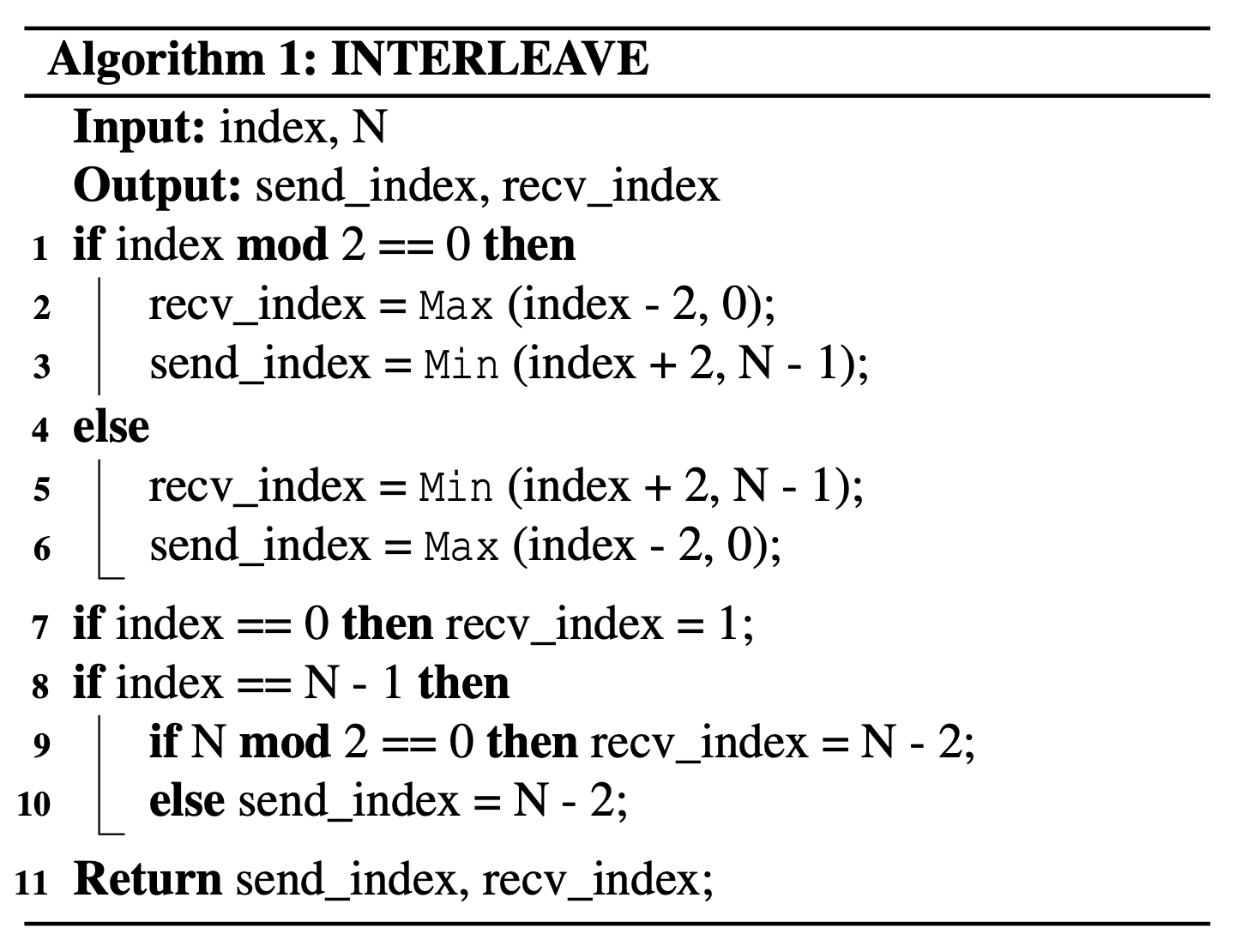
This complex pseudocode is easier to understand with visualization.
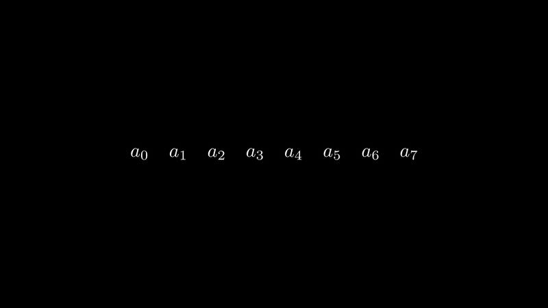
In the animation above, we first see that in Cannon’s algorithm, there’s an extremely long communication distance step.
To avoid ultra-long communication links, we thought of a ring data structure where the distance between any two neighbors is 1. If we flatten the ring onto a one-dimensional space, we achieve the interleave operation, implementing a movement scheme with a maximum link of 2. This greatly optimizes system communication efficiency.
Time complexity is reduced from O(n) to O(1).
Our discussion based on one-dimensional arrays naturally extends to two-dimensional grids. We perform interleave operations along both X and Y axes. In MeshGEMM, any single operation limits communication overhead to two hops.
The subsequent operations are not much different from Cannon’s algorithm. We adopt the same process of alternating movement and computation. The main steps of the MeshGEMM algorithm are:
- Initialization: Consider C=A×B. MeshGEMM splits A and B into sub-blocks
A_subandB_subalong two dimensions, forming N×N blocks distributed across cores. Each core receives one block ofA_subandB_sub. MeshGEMM then usesINTERLEAVEto initialize each core’s neighbor positions. - Alignment: Each core aligns with neighbors, ensuring that each core in the distributed system starts the matrix multiplication process with appropriate operands.
- Compute-shift loop: Each core executes N steps of communication and computation loops. At each step:
- Compute partial sum
C_sub = A_sub × B_sub + C_sub - Simultaneously, shift
A_subalong X-axis andB_subalong Y-axis to get newA'_subandB'_subfor the next computation (as shown in ③ of Figure 7) - After N steps, return the accumulated
C_sub
- Compute partial sum
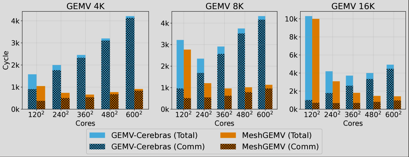
3.2 Operator Optimization - GEMV
The completion time of distributed GEMV mainly depends on an Allgather operation, which aggregates partial results from all selected cores and broadcasts the aggregated results back to all cores. Similar to GEMM, we analyze the same metrics.
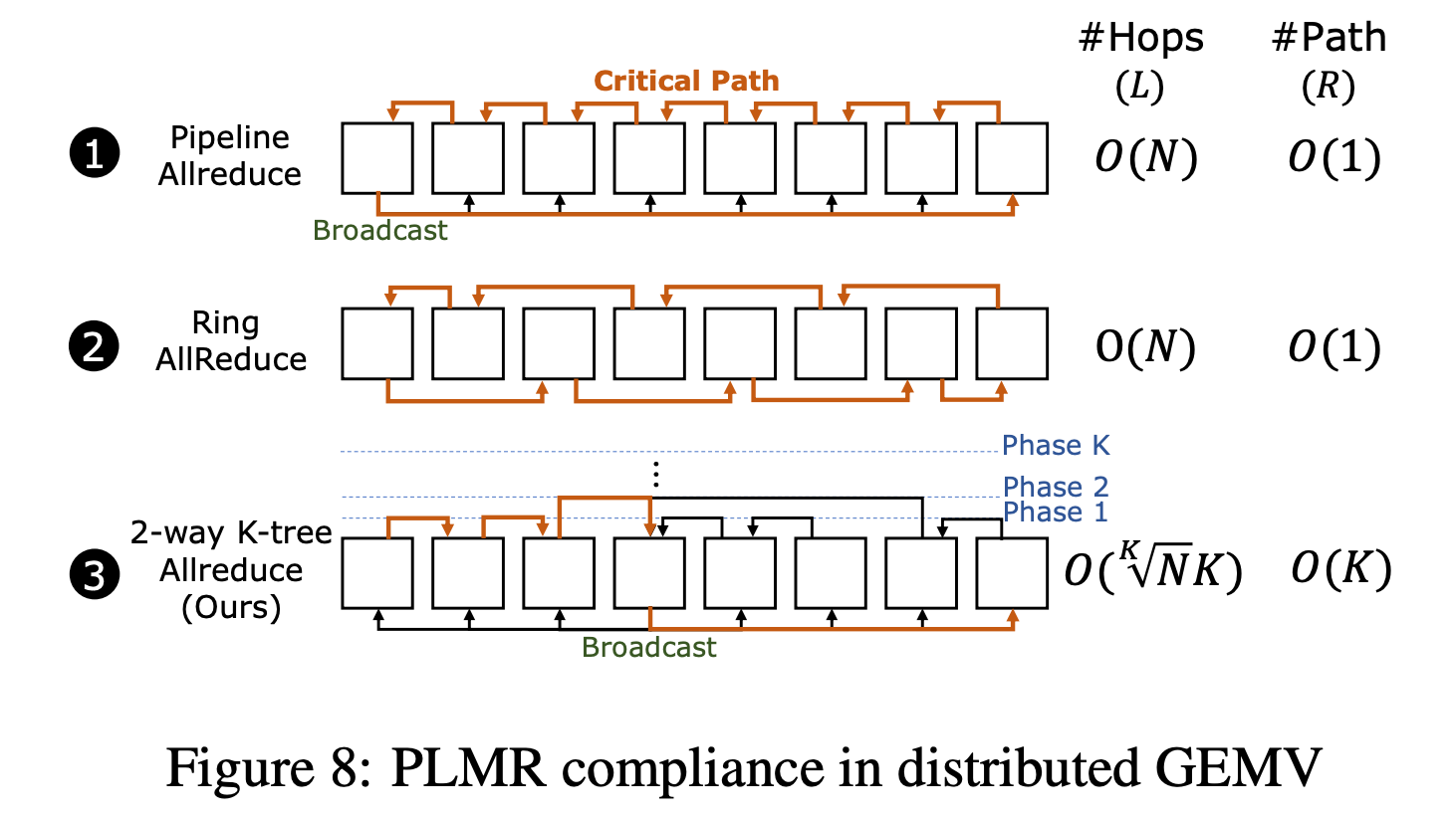
MeshGEMV is the only method that fully complies with the PLMR model:
Pipeline Allreduce: Commonly used in TPU cluster systems and Cerebras. It limits routing resource usage to O(1) per core (satisfies R). However, its longest aggregation path is from tail to head core, as shown by the red line, spanning O(N) critical path (violates L).
Ring Allreduce: Commonly used in GPU cluster systems as the default configuration. It limits routing resource usage to O(1) (satisfies R). However, it spans O(N) hops on the critical path (violates L).
2-Way K-Tree Allreduce: We build a balanced K-tree reducing from two directions; its longest aggregation path is from head or tail core to the tree root core. The critical path is $O(N^{1/k} × K)$, which can address L. The maximum communication paths per root core is O(K), which can satisfy R constraints by adjusting K.
MeshGEMV algorithm main steps:
- Initialization: Consider C=A×B, where A is a vector. MeshGEMV splits B into sub-blocks
B_subalong two dimensions, forming N×N blocks distributed across computing cores. For vector A, MeshGEMV splits along the vector length, forming N blocks distributed on one axis and replicating A on the other axis. Each core receives one block ofA_subandB_sub. Then determine which cores form a group at each stage based on the K-tree structure for efficient aggregation results. - Parallel computation: In this phase, each core independently performs local GEMV operation
A_sub × B_sub, computing their respective partial sumsC_sub. - Aggregation: The aggregation step mainly utilizes our designed 2-Way K-Tree Allreduce mechanism, specifically including:
- Stage 1: Intra-group reduction within each group, gathering results to each group’s root core, obtaining partial sums of
C_sub - Stage k: Further reduce results from stage (k-1) to root cores of each group in stage k
- After K repetitions, complete C can be obtained by concatenating
C_subfrom all K-tree root cores - (Optional) Depending on whether continuous GEMV operations are needed, broadcast operations from K-tree root cores downward may be performed
- Stage 1: Intra-group reduction within each group, gathering results to each group’s root core, obtaining partial sums of
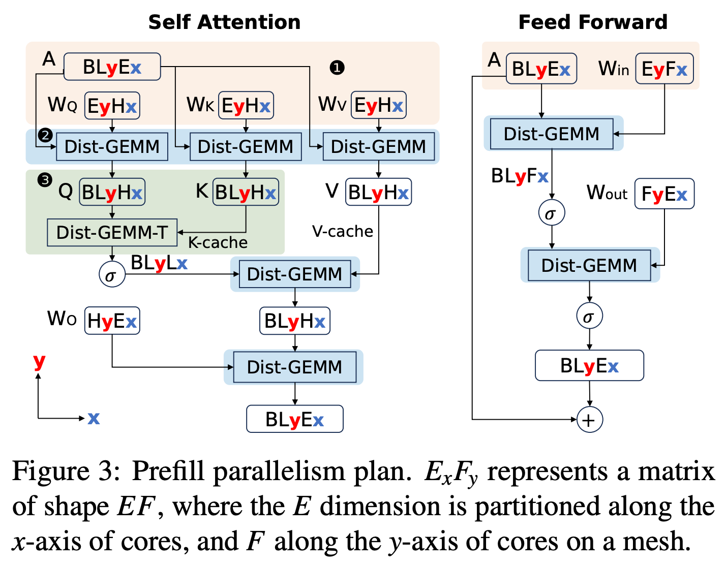
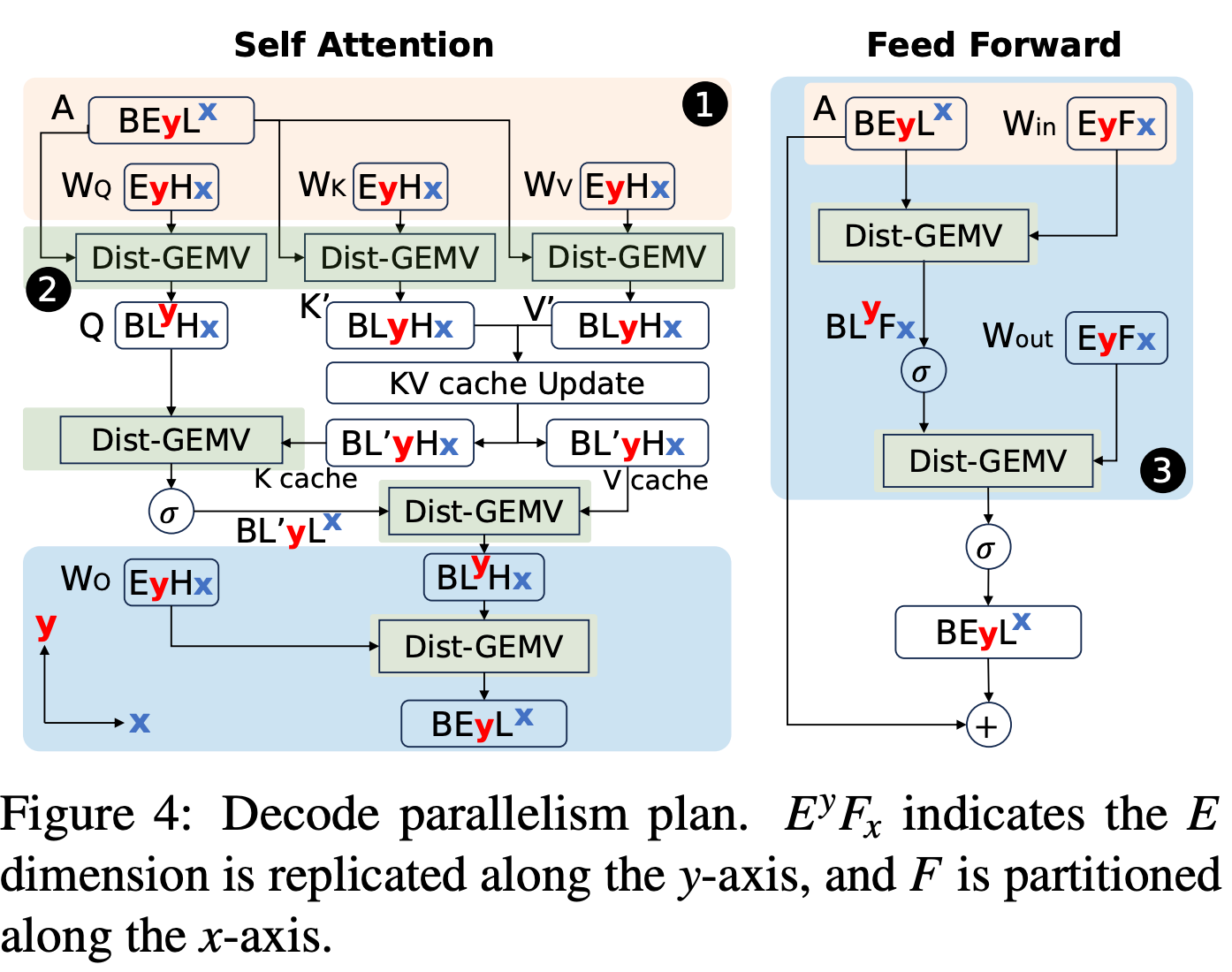
3.3 Model Layout
After handling operators, we next begin to layout the entire model, where Prefill and Decode have some different challenges:
- Multiple large matrices during Prefill require effective dimension partitioning to fully utilize all PEs, satisfying (P);
- Decode uses smaller matrices than Prefill, requiring careful parallelization;
- This phase mainly relies on GEMV operations, which are less compute-intensive than GEMM, resulting in short computation phases with limited ability to hide latency between communication;
- When Prefill and Decode continuously perform GEMM/GEMV, matrix transposition needs to be handled.
First, we proposed two different partitioning schemes.
Prefill partitioning scheme:
Decode partitioning scheme:
In Prefill partitioning: We partition the two dimensions of matrices along the X and Y axes of the PE array, achieving finer-grained, million-level parallelism than existing methods. The figure above shows the partitioning method for Self Attention and Feed Forward in the Prefill phase.
In Decode partitioning: When tensor dimensions are insufficient to achieve the high parallelism required for Decode, we replicate vectors in the orthogonal direction to data arrangement in LLMs. This method improves parallelism and ensures load balancing across all cores while avoiding additional communication operations, trading redundant storage for communication.
To eliminate matrix transposition, in Prefill, we designed transpose-free distributed GEMM. We proposed transpose-free operators, changing the communication direction, using transposed distributed GEMM (dist-GEMM-T) to compute Q@K^T during Prefill, avoiding the costly matrix transpose operation on NoC.
In the Decode process, since the operator bottleneck is in Allgather, redesigning the algorithm doesn’t bring benefits, so we pre-optimize model weight layout to avoid matrix transposition. Pre-optimizing model weight layout for Decode, directly reading transposed matrices onto the PE array, can eliminate matrix transposition in the MeshGEMV phase. Although this introduces overhead of rearranging weights between Prefill and Decode phases, with the super-strong communication capability on the NoC network, this overhead is almost negligible compared to generating one token.
3.4 Shift-based KV Cache Management
KV cache management on PLMR devices is also not simple, requiring storing large amounts of data on distributed cores while adhering to local memory constraints (M) and allocating KV cache computation to achieve high parallelism (P).
Simply put: We implemented an adaptive KV Cache storage scheme on 2D Mesh. Through dynamic balancing, on-chip memory utilization is more充分.
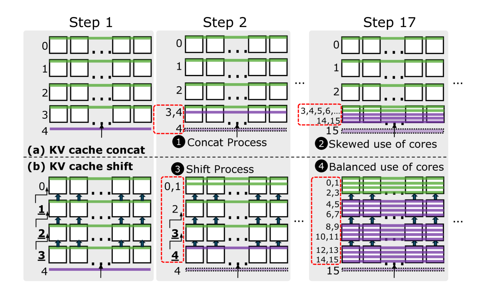
Our findings and solutions include:
- Existing concatenation-based management leads to core utilization: Current KV cache management methods mainly concatenate newly generated KV vectors to existing caches. While efficient on shared memory architectures, this concatenation operation leads to highly skewed core utilization on PLMR devices, as shown in ① of Figure 5, where only one core in a row is responsible for storing and computing newly generated KV vectors.
- Proposed shift-based management achieves balanced core utilization: We propose a shift-based KV cache management strategy that evenly distributes cache data across all cores. Instead of concatenating new KV cache vectors at the end, this method performs balanced shift operations, with each row transmitting the oldest KV cache data to the row above, as shown in ③ of Figure 5. This ensures even distribution of KV cache across all cores, addressing the M violation observed in the last row cores in concatenation-based methods.
4 WaferLLM Results
Through WaferLLM, we demonstrated the huge potential of Wafer Chips in LLM inference. We conducted comprehensive evaluations on Cerebras WSE-2, comparing with multiple state-of-the-art systems. Experimental results show that WaferLLM achieved significant breakthroughs in system performance, operator optimization, and energy efficiency.
4.1 End-to-End LLM Inference Performance
We first evaluated the end-to-end performance comparison of WaferLLM with representative systems, including the distributed memory architecture T10 system and the shared memory architecture Ladder system.
Performance improvement over T10 system:
- Short sequence generation tasks (input 4096/2048 tokens, output 128 tokens): WaferLLM is on average 160x faster, up to 180x
- Long sequence generation tasks (both input and output 4096/2048 tokens): WaferLLM is on average 36x faster, up to 48x
Although T10 considers memory constraints (M) and routing resource limitations (R) of PLMR devices, it cannot handle the core architecture of mesh NoC interconnects, thus unable to address different hop distances (L) or scale to millions of cores (P).
Performance improvement over Ladder system:
- Short sequence generation tasks: WaferLLM is on average 625x faster, up to 677x
- Long sequence generation tasks: WaferLLM is on average 312x faster, up to 342x
The Ladder system is designed for shared memory architectures and cannot adapt to PLMR device characteristics, resulting in inability to partition LLMs on millions of cores (P), expensive long-range NoC communication (L), inability to handle local memory constraints (M), and limited routing resources (R).
4.2 Operator-Level Performance Optimization
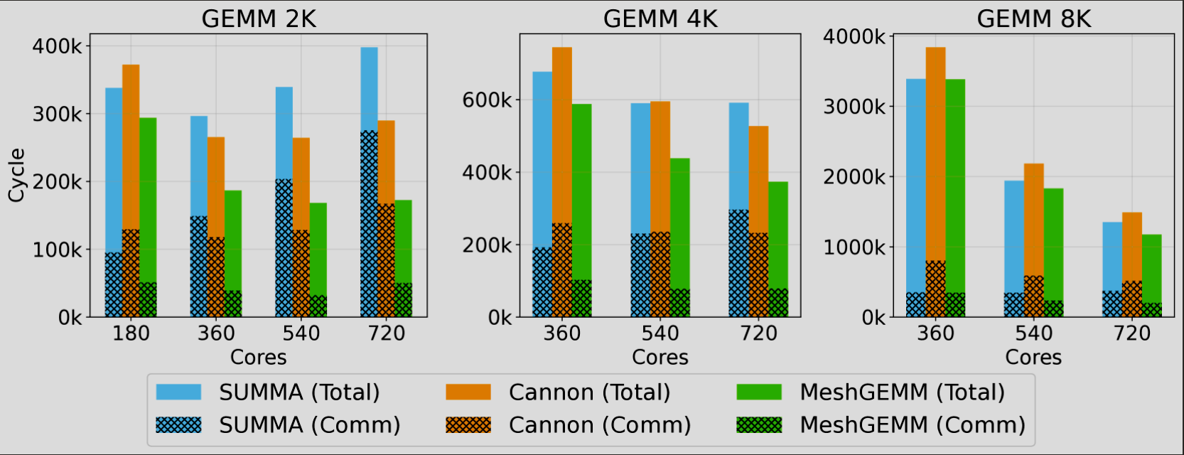
MeshGEMM Performance:
- 2-3x faster than Cerebras WSE’s default SUMMA algorithm
- Significant improvement over Cannon algorithm commonly used in supercomputers
- Maintains over 70% computational efficiency when scaling core counts, while SUMMA and Cannon efficiency drops below 50%
MeshGEMV Performance:
- 4-8x faster than Cerebras’s optimized default GEMV implementation
- Significantly reduces communication overhead through efficient bidirectional K-tree AllReduce
- As core count increases, communication cost only slightly increases, while baseline methods suffer severe performance degradation
Scalability Analysis: Our operators demonstrate excellent scalability across different core configurations. For large-scale matrix operations like GEMM 8K, computation becomes bandwidth-constrained rather than latency-constrained. Increasing core count can boost aggregate network bandwidth, resolving performance bottlenecks.
4.3 KV Cache Management Effectiveness
Shift-based KV cache management achieves huge improvements over traditional concatenation-based methods (like PagedAttention):
| Model | Concatenation Method (PagedAttention) | Shift Method (WaferLLM) | Improvement |
|---|---|---|---|
| LLaMA3-8B | 382 tokens | 137,548 tokens | 360x |
| LLaMA2-13B | 16 tokens | 6,168 tokens | 385x |
This significant improvement stems from the balanced core utilization achieved by the shift method, addressing the data skew problem caused by concatenation methods.
4.4 Performance Comparison with GPU
We conducted a fair comparison between WaferLLM (based on Cerebras WSE-2) and NVIDIA A100 running vLLM. Both are manufactured using TSMC 7nm process.
GEMV Operation Comparison:
- Performance improvement: MeshGEMV is 606x faster than cuBLAS GEMV
- Energy efficiency improvement: Energy efficiency is 22x higher than A100
This reflects the advantages of wafer-scale devices through massive on-chip memory bandwidth and wafer-scale connections (connecting on-chip memory) compared to GPU’s PCB-level connections (connecting off-chip HBM).
Complete LLM Inference Comparison:
| Model | WaferLLM(WSE-2) | vLLM(A100) | Performance Improvement | Energy Efficiency Improvement |
|---|---|---|---|---|
| LLaMA3-8B | 2,480 tokens/s | 78.36 tokens/s | 31.6x | 1.4x |
| LLaMA2-13B | 1,848 tokens/s | 47.86 tokens/s | 38.6x | 1.7x |
Inference Speed Breakthrough:
- LLaMA3-8B: Achieves decode speed of 2,700 tokens/sec/req
- QWen2-72B: Achieves decode speed of 840 tokens/sec/req
4.5 Performance Analysis and Limitations
While WaferLLM achieved significant performance improvements, we also observed some current limitations:
Performance degradation from GEMV to complete LLM: The 22x energy efficiency advantage of GEMV drops to 1.7x in complete LLM inference, mainly due to:
- Limited local SRAM (48KB) in WSE-2 cores, hindering efficient tensor parallelism
- Current LLM models optimized for GPU architecture, with narrow layer designs limiting layer placement on WSE-2 cores
Hardware maturity impact: As a second-generation product, WSE-2 cores cannot fully overlap memory access and computation, edge core utilization is insufficient, and long-range NoC communication overhead still exists.
Software stack limitations: Cerebras’s current software stack has limited optimization compared to NVIDIA CUDA, affecting overall performance.
Despite these limitations, WaferLLM still achieved order-of-magnitude performance and energy efficiency improvements. We expect performance to further improve as wafer-scale AI computing continues to mature and these limitations are gradually resolved.
5 What is Wafer?
Having covered the dry theoretical parts of the paper, let’s circle back to the opening question: What is Wafer?
Technically, it’s wafer-scale integration, an implementation approach for larger hardware; but actually from a systems perspective, it’s a rebalancing of computation, communication, and memory access ratios. Our past distributed system designs will once again be active on the Wafer stage.
Wafer’s emergence challenges our existing understanding of computing paradigms. Its unique PLMR characteristics require us to redesign algorithms and systems at the software level. MeshGEMM and MeshGEMV are just the beginning; there’s still vast research space for future optimizations for sparse matrices, convolutions, and higher-order tensor operations.
Wafer’s potential lies not just as a tool for AI acceleration, but possibly as a glimpse of future computing architecture—a new paradigm that merges “distributed” and “on-chip.” We can boldly speculate that as AI chips reach a fever pitch, all the Tensor Parallel, Data Parallel, Pipeline Parallel, and even popular Expert Parallel approaches we’ve thought about will equally return to their essence in the face of new architectures. Our thinking returns to the most basic and essential systems problem: “scheduling of computation, communication, and memory access.”
Every step forward in technology is a process of “repeatedly seeking balance.” Facing new “dynamics,” we must not only “adapt strategies to circumstances” but also remember the “essence.” Continuously exploring the balance between computation and communication, hardware and software, theory and practice.
So, looking back at my blog posts from recent months, I have many feelings. After DeepSeek appeared, I became numb and self-defeating for a while, but thinking from a systems perspective, I found that most solutions to problems in this world are quite far-fetched. Whether vLLM or sglang, they all propose solutions in special environments and assumptions. And the systems-level problems of “computation, communication, memory access” seem completely unsolved.
After completing the Wafer project, I may have truly touched the boundary of the MLSystem field: abstracting complex hardware structures and balancing various resource overheads. And this is the System I love most.